Through Silicon Vias - Enabling 3D MEMS integration
Through Silicon Vias (TSVs) are high-performance interconnect techniques and a key enabling technology for 3D integration of MEMS. Compared to 3D techniques such as flip chips, wire bonds, or package-on-package, the density of through-silicon vias is substantially higher, and the length of the connections is shorter.
TSV Approaches
TSVs are usually categorized as ‘Via-First’ or ‘Via-Last’, the main differentiator being that via-first take place before wafer bonding and are able to withstand temperatures of several hundred degrees. Via-last are post bonding, and typically the temperatures involved need to be low enough to prevent damage to back-end CMOS layers.
Each TSV type has its particular strength. Teledyne MEMS is pleased to offer silicon, copper, polysilicon, and other metal TSVs.
Silicon Via-First TSVs
Teledyne MEMS Via–First TSVs can use the trench fill (in-situ doped poly) as the conductor, or if larger vias are required, the conductive region can be the MEMs wafer itself, in which case the trenches are used only to provide isolation. This technology is available for both 150mm and 200mm wafers.
- Vias formed using bulk-silicon with oxide-filled trench isolation
- Smaller vias can be made with electrically isolated doped poly
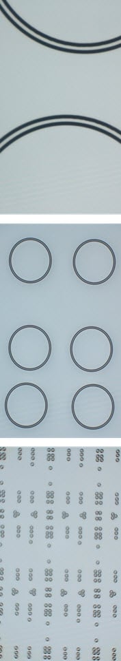
- TSV is standard with the Teledyne MEMS inertial sensor platform
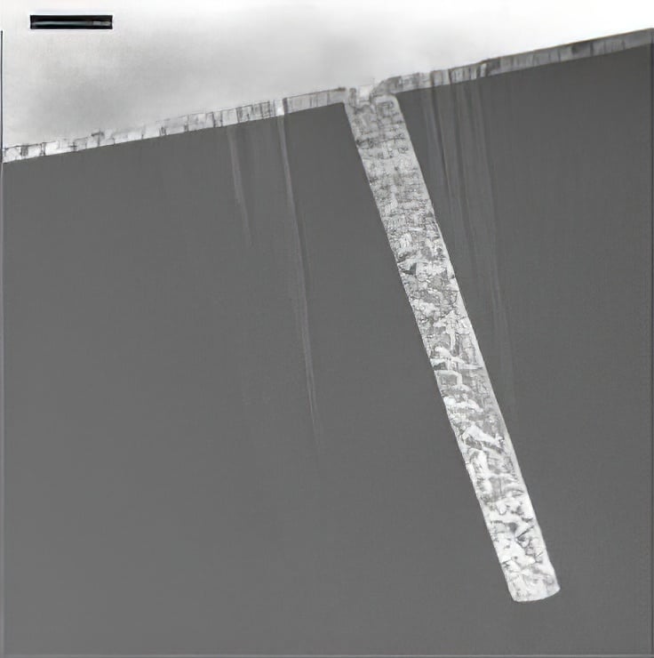
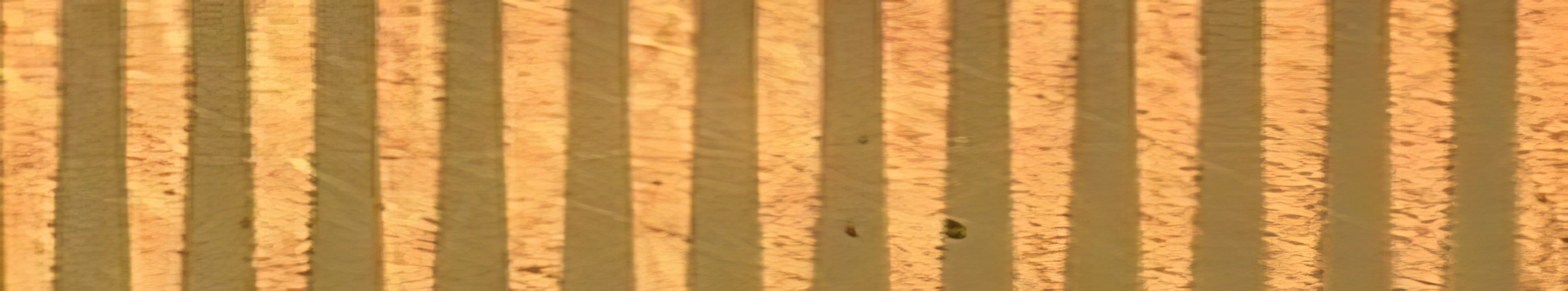
Copper-filled 5µm wide trench before planarization
Copper Via-Last TSVs
- Filled using low temperature electrochemical process.
- 5um CD on thinned wafers – post-bonding
- This process is available for 200mm wafers only
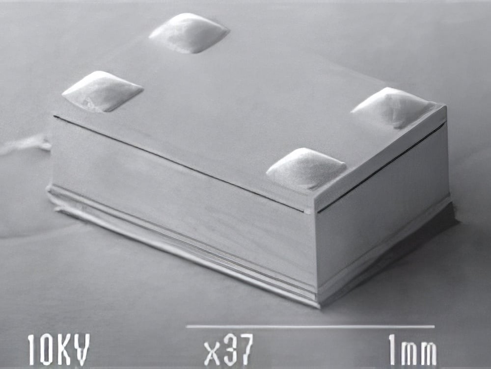
Teledyne’s Via-Last technology utilizes copper vias, filled using the aveni low-temperature electrochemical process. This technology produces perfect filling of 100 µm vias only 5µm diameter, which connect to the outside world through a copper redistribution layer and Ni/Au UBM.
Wafer Level Packaging
Surface mountable 3D ICs use wafer level packaging for dramatic size and form factor reduction with corresponding cost reductions, making them ideal for mobile applications. Teledyne MEMS offers advanced I/O options including µBGA, solderable pads, or standard pads for stacked die and co-package designs, with hermetic seals for oscillators, pressure and image sensors, and non hermetic for RF filters, microfluidics and Si microphones.
Learn more about application we support.
Teledyne MEMS Capabilities
We blend MEMS applications experts together with process performance champions to design process flows for robust, cost-effective fabrication to match customer requirements. Our project teams strive for deep insights to their customers’ needs and close communications throughout the relationship.

Do you have any questions?
Select Teledyne as your partner to move your MEMS device from concept to mass production.
Contact usStay connected
The MEMS industry is evolving quickly with new innovations, applications, and events. Subscribe to our newsletter and we’ll help you keep up to date with the latest developments
Subscribe