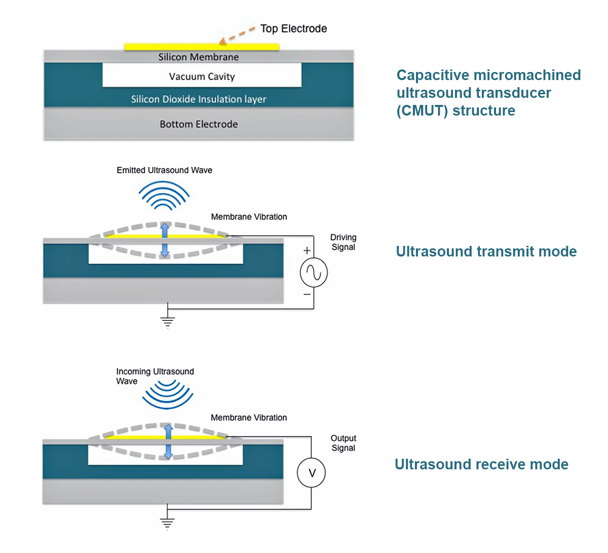
CMUT / Ultrasound
Capacitive micromachined ultrasonic transducers (CMUTs) are MEMS-based structures that can be used to generate and sense acoustic signals in the ultrasonic range. CMUT systems offer advantages miniaturization, superior imaging resolution, and high temperature reliability, conditions where conventional ultrasound transducers tend to fail.
Innovation and advantage
Today they offer significant advantages over conventional PZT transducer materials, which have dominated ultrasound examination products.
- CMUTs offer better acoustic matching to the propagation medium, resulting in wider immersion bandwidth and improved image resolution, with frequency range from 500 kHz to 50 MHz, tunable by precision dimensional control
- CMUTs are lead free, ROHS compliant, with no toxic materials, which is especially advantageous for invasive ultrasound, unlike lead based PZT devices
- CMUTs can be integrated with electronic circuits in chip-scale packages, leading to smaller form factors and more reliable and robust designs
CMUTs: A natural solution for 3D imaging
With higher sensitivity and wide bandwidth operation, CMUTs make an ideal solution for photoacoustic imaging. The easier manufacturing and lower production costs of silicon micromachining can replace the labor-intensive, element-based assemblies of conventional PZT handheld linear arrays.
Imaging Applications
Today's ultrasound technology covers a wide range of measurements, diagnostic, and other applications, e.g. from non-destructive testing to medical ultrasound imaging or from surveillance in process plants to distance measurement.
- Photoacoustic imaging combines the high-contrast and spectroscopic-based specificity of optical imaging with the high spatial resolution of ultrasound imaging
- High intensity focused ultrasound (HIFU) is a treatment that aims to kill cancer cells with high frequency sound waves.
- Guidance for therapeutic ultrasound
- Affinity sensor for immunosensing
- Ultrasound microscopy
CMUT Fabrication at Teledyne MEMS
We offer advanced prototyping, development and volume manufacturing services for CMUTs, both for components and for complete module assemblies. Our patented CMUT design uses a doped Silicon-on-Insulator (SOI) and wafer bonding fabrication method composed of semiconductor layers, insulator layers, and metal layers.
Conventional doped silicon may be used as the electrode layers. Other suitable semiconductor materials such as silicon carbide may alternately be used for the electrode layers. The insulator can be made of silicon oxide, silicon nitride, or other suitable dielectrics.
Other MEMS Applications
Teledyne MEMS is committed to innovation, developing new sensing technologies to serve areas like the rapid growth in diverse industries from microfluidic devices for cancer research and implantable medical devices to optical cross-connects for telecom, gyros in game controllers, and pressure and inertial sensors for automotive applications.

Do you have any questions?
Select Teledyne as your partner to move your MEMS device from concept to mass production.
Contact usStay connected
The MEMS industry is evolving quickly with new innovations, applications, and events. Subscribe to our newsletter and we’ll help you keep up to date with the latest developments
Subscribe