Photolithography
Virtually all MEMS and microfabricated devices start with a pattern on the wafer.
This patterning is used to selectively isolate certain areas of the die for deposition, etching, doping and other activities.
Expose
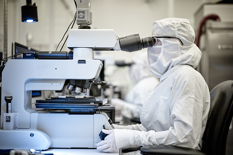
Teledyne MEMS uses both steppers and contact aligners to provide various photolithography capabilities.
ASML PAS 5500/60B I-line 5X reduction stepper
- Submicron resolution: 0.45 µm
- Single machine overlay: 90 nm (3 sigma)
- 3” to 8” fully automatic tool
- 55 wafers/hour throughput (6”)
- UDOF > 1 µm @ 0.45 µm with NA=0.54
- Minimum features: 0.5 µm with CD uniformity: 60 nm (3 sigma)
Contact Aligner 1:1
- Minimum features: 1 µm (vacuum contact mode) & 3 µm (proximity mode)
- Alignment accuracy: 1 µm (frontside align) & 3 µm (front to backside align)
- CD uniformity: 0.1 µm (1 sigma)
Coat & develop
The YES LP-III vacuum oven is used for hexamethyldisilazane (HMDS) vacuum vapor priming to improve the coverage and adhesion of the photoresist to the wafer. Clean wafers are dehydrated through a series of 150C heated evacuations and dry nitrogen refills. HMDS vapor then flows into the evacuated chamber forming a monolayer on the wafer surfaces.
Automated SVG 8600 coat & develop tracks
- 4”/6”, transparent wafer compatible
- Positive resists thickness 1-15 µm
- Thickness uniformity control down to 1% for thin resist
- Puddle/spray develop with developer chemical temperature control
Stand-alone Solitec coat & develop tools
- Spun on lift-off layers, negative resists including SU-8, thick resists for electroplating
- Square substrates, small substrates
- Spray develop
- Metal ion bearing or metal ion free developers
Accuracy & processes
Our Bromont facility’s 200 mm MEMS line has been installed to provide capacity for higher volume production, and to support wafer level bonding of MEMS to 200 mm CMOS wafers. There is a high degree of commonality between our 150 mm and 200 mm MEMS lines, and most applications which run on 150 mm can be transferred to 200 mm if required.
Lithography
- 5X front to front (ASML) 0.35 µm feature, 0.1 µm accuracy
- 5X front to back (ASML) 0.35 µm feature, 0.2 µm accuracy
- 1x front to front 3.0 µm feature, 0.5 µm accuracy
- 1x front to back 3.0 µm feature, 0.75 µm accuracy
Positive & negative resists
- Dry film lamination of photo-definable thick polymers
- Spin coating of thin and thick photoresists and photopolymers
Teledyne MEMS Capabilities
We blend MEMS applications experts together with process performance champions to design process flows for robust, cost-effective fabrication to match customer requirements. Our project teams strive for deep insights to their customers’ needs and close communications throughout the relationship.

Do you have any questions?
Select Teledyne as your partner to move your MEMS device from concept to mass production.
Contact usStay connected
The MEMS industry is evolving quickly with new innovations, applications, and events. Subscribe to our newsletter and we’ll help you keep up to date with the latest developments
Subscribe