MEMS for Industrial Sensors
We live in an increasingly connected world. Every imaginable device will eventually be connected to a cloud-based data system, to sense everything from air quality to livestock fertility, and to provide real time data to users. This trend spans consumer and industrial environments and is spawning countless new applications and infrastructure spending. Sensors are becoming ubiquitous and are the common foundation for each and every one of these new applications.
Advanced Industrial Sensor Design and Manufacturing
Efficient MEMS design and manufacturing are the keys to cost-effectiveness of sensor applications. Purpose-designed MEMS sensors hold the key to mass adoption, deployment and ROI for these massive development efforts, applied variously to consumer devices, internet of things (IOT) products, or business-to-business (B2B) networks.
Pressure Sensors
Pressure sensors are among the most widely used MEMS-based devices and can be found in industrial, automotive, aerospace, defense and consumer applications. There are a variety of techniques to create pressure sensors but nearly all device functions are either capacitive or piezo-resistive. Pressure sensors also have an enormous range of sensing values and robustness determined by the application and its operating environment.
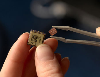
Inertial Sensors
Inertial sensors are used to measure aspects of physical movement like thrust, velocity, angle and direction, and are widely used in consumer applications like smart phones, game consoles, automotive air bag systems and GPS displays.
However, the greater inertial sensor market includes oil and gas exploration, geological survey equipment, medical devices and aerospace. Regardless of application, MEMS-based inertial sensors require complex and precise etching techniques to create fine geometries that are consistent across the wafer.
Gas Detection
The application of MEMS technology has allowed Metal Oxide Gas Sensors to be mass-produced at the wafer level. Silicon wafer manufacturing allows for cost reduction and scalability to large volumes.
Our process capabilities enable the creation of gas sensor devices suitable for precise measurement of Carbon Monoxide (CO) and a wide range of Volatile Organic Compounds (VOCs) such as Ethanol, Acetone and Toluene. Sensor arrays and comparative signal processing can increase selectivity to target specific gasses.
Metal Oxide MEMS Platform Features:
- Integrated micro-heater - platinum thin films, refractory metals, electrically isolated from the sensor
- Interdigitated sensor electrodes
- Metal oxide sensing film - catalyst doping for greater sensitivity
- Thermal isolation membranes: low-stress dielectric films, backside or front side airgap
MEMS-based gas detection provides dramatic size reduction, a reduction in power consumption, and the ability to increase functionality and selectivity through the use of multisensory arrays on a single chip.
Wafer based Metal Oxide gas sensors are suitable for integration into a wide variety of gas sensing applications – largely driven by health and safety considerations, including environmental monitoring, biological research, and industrial control.
Wafer-level packaging for Inertial Sensors
The Teledyne MEMS wafer-level packaging (WLP) process platform provides an all-in-one customer solution integrating wafer level fabrication, hermetic packaging and through-silicon-via (TSV) architecture. Our established design kit reduces initial development cost, ultimate manufacturing component cost, footprint, thickness and weight, while simultaneously providing improved electrical performance, reliability, and extensibility into 3D IC designs.
Our WLP process platform can be used for a variety of inertial sensors. The WLP is a proven, cost-effective solution for applications requiring high accuracy, low-noise mechanical sensing by devices operating across wide frequency ranges and requiring high vacuum encapsulation.
Features include:
- Insulated Through Silicon Vias (TSV) Thick silicon device layer (60 microns standard) for high comb finger capacitance
- Lead-free solder ball grid array
- Wafer level bonding processes optimized for getter film activation and hermetic sealing
Other MEMS Applications
Teledyne MEMS is committed to innovation, developing new sensing technologies to serve areas like the rapid growth in diverse industries from microfluidic devices for cancer research and implantable medical devices to optical cross-connects for telecom, gyros in game controllers, and pressure and inertial sensors for automotive applications.

Do you have any questions?
Select Teledyne as your partner to move your MEMS device from concept to mass production.
Contact usStay connected
The MEMS industry is evolving quickly with new innovations, applications, and events. Subscribe to our newsletter and we’ll help you keep up to date with the latest developments
Subscribe